
[ad_1]
Reducing the carbon footprint of the manufacturing course of for photo voltaic modules is essential to creating the expertise actually sustainable. Huasun’s streamlined heterojunction (HJT) manufacturing led to the certification of its newest product as ultra-low-carbon photo voltaic.
Solar generates zero-emissions vitality, however considerations are rising in regards to the environmental and useful resource affect of PV module manufacturing. In at the moment’s market, the main focus has shifted to evaluating the general carbon footprint of photo voltaic modules. This shift will be attributed to the more and more obvious results of local weather change, coupled with considerations about environmental and human well being points, in addition to useful resource shortage.
Assessing the carbon footprint of a photo voltaic module is a crucial facet of this analysis, providing a concise metric for evaluating manufacturing strategies. Low carbon footprint numbers imply manufacturing processes that require much less assets on Earth, displaying a dedication to environmental sustainability.
The want for silicon
The manufacturing technique of photo voltaic cells and wafers requires giant quantities of vitality in a vital collection of processes. Technological advances are important to assist shift using photo voltaic vitality assets to greener and greener territory.
An necessary vitality requirement for many varieties of standard PV merchandise is the manufacturing of polysilicon, which requires excessive temperatures to refine the purity required for silicon wafers utilized in photo voltaic. The course of includes heating quartz sands in a furnace. The polysilicon is then fashioned into ingots, that are minimize and sliced into silicon wafers to be used in crystal merchandise. The calls for of silicon within the photo voltaic business are excessive, and photo voltaic merchandise typically should be over 99.9999%, referred to as 6N purity. It is of upper purity than metallurgical silicon.
The newest photo voltaic manufacturing utilizing crystalline silicon consists of both a mature course of referred to as passivated emitter and rear contact (PERC), and two new processes or applied sciences referred to as tunnel oxide passivated contact (TOPCon) or HJT photo voltaic cell expertise. Each manufacturing course of has its personal advantages for various stakeholders, and evaluating and contrasting every technological course of is past the scope of this text.
When photo voltaic modules are evaluated by conventional metrics, parts together with effectivity, value, and reliability are widespread benchmarks. However, the carbon footprint of a module is an extra focus for a lot of stakeholders, and is already topic to regulation in lots of nations, together with France and Korea. In crystalline photo voltaic, the place the commercial provide chain is very centered, just one manufacturing approach has a cleaner manufacturing course of: HJT.
Comparison of carbon
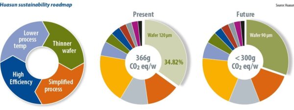
In July 2023, Huasun Energy launched a carbon footprint report for its HJT photo voltaic module, the Himalaya Series G10-144, with the report licensed by TÜV Rheinland. The HJT module discovered a results of 366.12 g of CO2 equal emission per watt. This makes it one of many first confirmed photo voltaic modules to fall under 400 g/W CO2 corresponding rating, and it’s seen that it falls into the class of the business thought-about as extremely low-carbon photo voltaic.
The distinction in comparison with different applied sciences is large. While every producer’s personal carbon footprint will rely upon the native mixture of electrical energy used within the full manufacturing course of, extensive ranges have been established in business studies. A examine by Fraunhofer ISE introduced on the 2022 World Conference on Photovoltaic Energy Conversion in Milan revealed the specs that suggest a typical glass-glass photo voltaic module made in China, the place greater than 85% of PV manufacturing in world happened, with a carbon footprint of about 750 g/W CO2 equal. That means Huasun’s newest module has virtually half the carbon emissions.
Advantages of HJT
Huasun’s HJT module makes use of silicon wafers with a thickness of 120 micrometers. That compares to a typical thickness of 150 micrometers in different crystalline silicon applied sciences comparable to PERC, thus delivering big financial savings in uncooked, energy-intensive materials. In addition, Huasun CTO Wang Wenjing defined that HJT expertise is, typically, friendlier to the silicon wafer: extra ingots can be utilized. Basically, that is as a result of different applied sciences minimize a photo voltaic cell after it is made, whereas HJT tech makes use of a half wafer earlier than the photo voltaic cell is made, which means a small portion of the wafer is faraway from the an ingot.
“In the previous, after we minimize a sq. ingot from a cylindrical ingot, the internal half was despatched again to CZ. [Czochralski] furnace that may be reworked into one other ingot. But in HJT cell, we will minimize the sting half to get half Si items. So we will use the sting function … to get extra wafer items from the identical ingot,” Wang stated. This leads to cheaper silicon wafers and extra environment friendly use.
The vitality financial savings from HJT are greater than wafer thickness financial savings and environment friendly use of ingots. HJT makes use of decrease temperature manufacturing processes and a less complicated manufacturing course of.
Huasun labels the method a “four-step” technique, and consists of clearing and texturing, bifacial chemical vapor deposition (CVD), bifacial bodily vapor deposition (PVD), and a remaining printing step. on the display. At every stage, the vitality requirement is lower than 200 C – a lot decrease than the 800 C to 1000 C required by different photo voltaic modules. For instance, the method utilized in TOPCon expertise can contain 10 or extra steps. In addition, decrease temperatures end in fewer cracks and defects, which improves manufacturing course of yield and effectivity.
This article seems within the new Huasun Corporate Edition, launched on April 10, 2024. Read the total version right here.
This content material is protected by copyright and is probably not reused. If you wish to cooperate with us and wish to reuse a few of our content material, please contact: [email protected].
[ad_2]
Source link
