
[ad_1]
EnPV GmbH, a subsidiary of German power supplier EnBW Energie Baden-Württemberg AG, has unveiled a photo voltaic cell primarily based on n-type tunnel oxide passivated contact (TOPcon) know-how and a brand new sort of back- contact structure, described as self-aligned back-contact (SABC) know-how.
“Common interdigitated back-contact (IBC) photo voltaic cells require an interdigitated sample that’s not homogeneous in nature and should shield the again aspect of the wafer throughout sure manufacturing steps,” the EnPV CEO , Massimo Centazzo, stated. pv journal. “Our SABC cell manufacturing avoids the masking of the again floor construction and, whereas utilizing laser-structuring as an alternative, manages the part insulation with none further devoted course of steps.”
Centazzo defined that part insulation consists of “reliably” insulating p- and n-phase from one another by means of a by-product of different course of steps, which explains why it’s “self-aligned.”
“The use of two methods, laser processes for structuring and self-aligned part insulation, results in a dramatic simplification of the manufacturing course of in comparison with every other back-contact cell course of,” the CEO stated. . “Although nonetheless permitting greater cell effectivity, SABC cells are produced at a decrease price than TOPCon and heterojunction (HJT) cells.
The producer claims that the brand new again contact know-how can simply be utilized in current TOPCon cell manufacturing traces, with the improve requiring the addition of a wet-chemical course of, a step within the course of. -laser construction, deposition of an etch-barrier and bodily vapor deposition. -based deposition of doped amorphous silicon for n-contact.
“Our technique doesn’t require a devoted trench to insulate the poly-Si layers of reverse polarity,” Centazzo continued to say. “Instead, the undercut of the ditch wall separates the 2 polarities, the place the primary p-type poly-Si layer lies above the ditch, whereas the second n-type poly-Si lies beneath the ditch.”

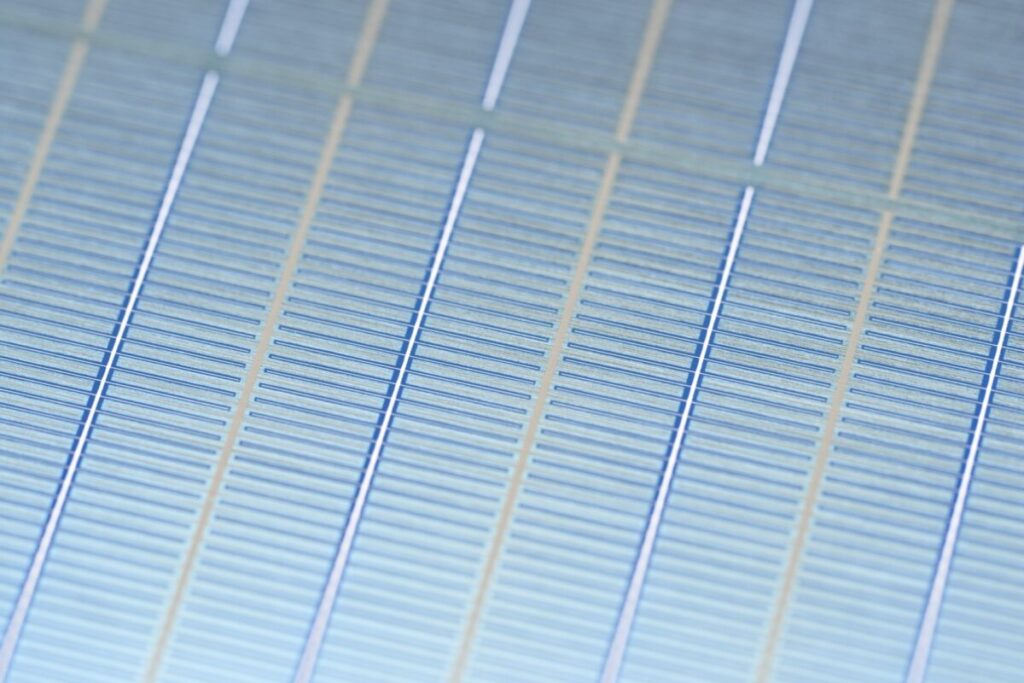
Image: EnPV GmbH
Under the undercut, which is made by moist chemical trench etching, no poly-Si is deposited in the course of the bodily vapor deposition (PVD) course of. The n-type poly-Si additionally covers the p-type poly-Si emitter forming a low resistive tunneling contact, as a result of each poly-Si layers are closely doped with a dopant that focus above 1,020 cm3. The n-type poly-Si layer covers the complete floor and permits using the identical metallization technique for each polarities, in line with the producer.
Centazzo additionally defined that the SABC goal course of began with texturing and spraying boron on the back and front. “A aspect borosilicate glass (BSG) etch adopted by alkaline etching of the boron emitter on the again prepares this floor for poly-Si deposition,” he highlights. “Instead of boron diffusion forming the entrance floating emitter (FFE), a phosphorus diffusion forming the entrance floor area (FSF) or an un-diffused floor can be utilized for the SABC course of move as nicely.”
Alkaline moist chemical etching strips the poly-Si on the entrance aspect as much as the BSG layer and on the again etch the p-type poly-Si within the uncovered areas. Back etching not solely removes the poly-Si layer, but in addition etches the silicon base vertically and laterally, creating an undercut on the floor. After the etch barrier and BSG removing and development of a second interfacial oxide, the subsequent deposited n-type poly-Si in PVD can’t cowl the complete again floor.
“With the extra directional deposition technique, the doped silicon is especially deposited on the vertically uncovered surfaces, which aren’t shaded by the undercut,” Centazzo emphasised. “Therefore, on the backside of the ditch n-type poly-Si types a passivating contact however there’s additionally an n-type poly-Si above the p-type poly-Si that types a tunnel junction to the emitter .The shadow aspect of the channel wall insulates the 2 passive contacts, with out the necessity for extra processing steps comparable to structuring, native etching or masking.
The manufacturing course of is then completed with excessive temperature annealing, crystallization of poly-Si layers and activation of dopants, normal passivation with aluminum oxide (AlOx) and silicon nitride (SiNx), and metallization by display printing. “Since the n-type poly-Si consists of the faces of the identical passivating contacts, the identical screen-printing paste can be utilized in a single printing step for a similar polarities,” Centazzo emphasised. .
He believes that SABC TOPCon cells will probably be cheaper than typical TOPCon cells.
“We count on an enchancment in effectivity when migrating from TOPCon to SABC of greater than 0.5% absolute on the cell stage, and a further 0.7% on the module stage resulting from decreased cell loss -to-module in back-contact modules in regular modules,” he added. “The price of conversion from cell to system quantities to €0.75 ($0.83)/W, whereas in an SABC-based system, resulting from elevated module effectivity, it decreases to €0.71/W, with the manufacturing price for the cells decreased from €0,100 /W to €0.85/W. Overall, a system primarily based on SABC modules prices €0.80/W, which is about 6% cheaper. than one with TOPCon cells.
The novel cell idea has a know-how readiness stage (TRL) of 6. TRL measures the maturity of the know-how elements for a system and relies on a scale from one to 9, with 9 which symbolize mature applied sciences for full industrial software. It can transfer to TRL-grade 8 provided that applied on a pilot manufacturing line in a mass manufacturing setting, in line with the corporate.
EnBW is at present dedicated to funding the event of SABC cells, nevertheless the industrialization technique remains to be beneath dialogue. “As EnBW’s territory of entrepreneurial actions is historically Germany and Europe, the place the manufacturing of PV is declining, the seek for appropriate companions for the industrialization of SABC ought to be expanded past Europe,” stated Centazzo, who introduced that EnPV is at present assessing launch alternatives. SABC’s cell factories are positioned on the planet’s hotspots of PV manufacturing, specifically the USA, India, and China.
“We envision elevating a pilot line later in 2025,” he concluded. “No choices have been made on which accomplice has been taken but.”
This content material is protected by copyright and will not be reused. If you wish to cooperate with us and wish to reuse a few of our content material, please contact: editors@pv-magazine.com.
Popular content material

[ad_2]
Source link